0 Abstract
System clocking is a basic setting when using this type of microcontroller. Information will be provided on how this is done by software. Various steps will be described that have to be taken to set the MCU to an appropropriate clock frequency including measurements with respective equipment to check clock accuracy.
1 Various sources for the clock signal
In the STM32F4 MCU there are 3 possible way of generating a clock signal:
- Internal High-Speed-Oscillator (HSI) with 16MHz fixed frequency
- External High-Speed-Oscillator (HSE) normally from 8 to 25 MHz frequency (crystal based)
- PLL frequency derived from either HSI or HSE clock signal.
When you startup the system by supplying VDD the internal oscillator (HSI) is switched as clock source. Which clock you are about to use afterwards is defined in RCC->CR (Clock Control Register):
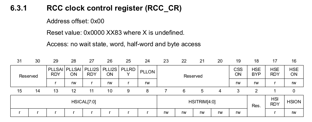
You can see two bits that work identically for HSI respectively HSE 16 bits apart in the same register: An “ON”-bit and a corresponding “RDY”-bit. First you power the oscillator of your choice by setting the “ON” bit to “1”.
1.1 Activate HSI
RCC->CR |= (1 << 0);
1.2 Activate HSE
RCC->CR |= (1 << 16);
After being switched “on” these oscillators need a short period of time until they are ready for use. This is checked in a loop by polling the respective flag bit:
while ((RCC->CR & (1 << 1) == 0); //Check HSI ready
while ((RCC->CR & (1 << 17) == 0); //Check HSE ready
1.3 Using PLL as clock source
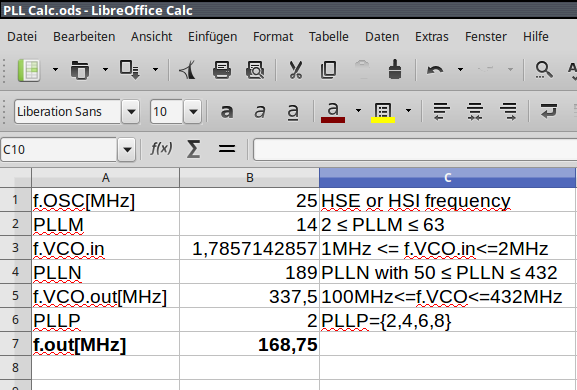
Besides using HSI oder HSE stand-alone, STM32F4 MCU allows the developer to apply an onboard PLL synthesizer to work as the primary clock source for the system. This might lead to a mac. clock frequency of 168 MHz. All settings are done by software, so you are not in danger, like with the AVRs, to “defuse” a controller. Software definition implies several steps because PLL setting involves definition of various parameters.
These parameters are named by the Alphabet, starting with PLLM, PLLN, PLLP and PLLQ.
Their frequencies are derived successively from the respective predecessor, the chain starts with PLLM. Provided we use 8 MHz HSE as input source, we have to modify PLLCFGR register. These steps are defined as:
//Set PLLM
RCC->PLLCFGR &= ~0x3F; //1st reset bits
RCC->PLLCFGR |= 4;     //2nd define VCO input frequency
                       //= PLL input clock frequency (f.HSE) / PLLM with 2 ≤ PLLM ≤ 63
                       //-> f.VCO.in = 8MHz / 4 = 2MHz
VCO input frequency is derived from HSE and divided by 4. This leads to f.VCO.in = 2 MHz which is fine because the boundaries are 1MHz <= f.VCO <= 2MHz (Ref. manual pages 163, 164).
Next is PLLN which is a multiplication and leading to VCO output frequency::
//Set PLLN: PPLLN defines VCO out frequency
RCC->PLLCFGR &= ~0x7FC0; //1st Reset bits 14:6
RCC->PLLCFGR |= (100 << 6); //2nd define f.VCO.out =
                             //f.VCO.in * 100 = 200MHz
With PLLP we define the PLL output frequency for modules like the USB interface. Certain limitations are to obeyed here, e. g. for USB frequency must be exactly 48MHz.
//Set PLLQ. PLLQ = division factor for USB OTG FS, SDIO and random number generator clocks
RCC->PLLCFGR &= ~(0b1111 << 24); //Reset bits 27:24
RCC->PLLCFGR |= (8 << 24); //PLL-Q: f.VCO.out / 8 = 25MHz
Nest step: We have to activate the PLL:
RCC->CR |= (1 << 24); //Activate PLL, Bit 24
while ((RCC->CR & (1 << 25)) == 0); //Wait until PLL is ready Bit 25
And finally the frequencies for the various bus systems and bridges must be set. For limitations see reference manual!
//Division of clock signal for bus system
RCC->CFGR |= (0b1001 << 4) //AHB divider: 100MHz / 4 = 25 MHz
| (0b100 << 10) //APB1 divider: /2
| (0b100 << 13); //APB2 divider: /2
Finally, not to be forgotten, PLL must be set as clock source for the MCU:
RCC->CFGR |= 0b10; //Switching to PLL clock source
Then you are ready to go!
Just another annotation: Onboard flash memory has to be configured as well. In Flash access control register (FLASH_ACR) the waitstates for FLASH memory have to be set. My rule of the thumb is:
- 1 WS for f=50MHz
- 2 WS for f>=100MHz
FLASH->ACR |= 0b010; //2 wait state for 100 MHz
If you want to experiment, write a short program that makes a LED blink and test it with various PLL settings up to 168 MHz. Just check if the program works. If the software hangs, try to increase memory waitstates!
Demo code for the “Black Pill” board (STMF411) can be found on my Github repo: Link.
BTW: I have created a little spreadsheet that can help calculating the various register. Click to download.
Hope you enjoyed the lesson. C U!
All rights reserved by Peter Baier, Bad Bergzabern, Germany (https://micromaker.de).