0 Abstract
In this chapter of our online course we will see how Alternate Functions (AF) in the STM32 MCUs are programmed and used. Later we will measure the clock frequency by activating the respective “AF” and put out main clock frequency via an external pin to measure it. Alternate functions are important when certain ports should be used outside the standard “inupt” or “output” featuring, for example as ports for I²C, SPI or so.
1 Alternate Functions in the STM32 MCU
As in AVRs in STM32 MCUs as well, you can assign different functions to a number of the controller’s pins. In STM32 this assignment is, as in AVRs, not 100% deliberate, certain pins are reserved for certain functions. And one pin can be assigned to more than one function but only one by a time.
Assigning a pin to an alternate function is a two-step process.
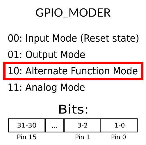
First, you have to configure a pin as “AF”:
Second, you have to define what alternate function is assigned to that respective pin. To determine this selection, there is a large table to be found in datasheet, called the “Alternate Function Table“. You can find that beginning on p. 62 and ending on p. 70 of the datasheet. Just have look to a small excerpt of this very large table:
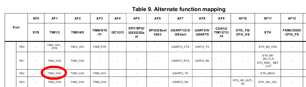
With this example we want to assign Channel 3 of Timer 2 to pin PA2:
First we have to define PA2 as “alternate function” using MODER register:
GPIOA->MODER |= (0b10 << (2 << 1));
Next step is that we have to look up the respective “AF”-code in the alternate function table. This is “AF1” for our intended purpose.
To map this “AF1” to pin PA2 another register (or to say more exactly “one of 2 possible registers”!) is needed: The GPIO alternate function registers (AFRL and AFRH):
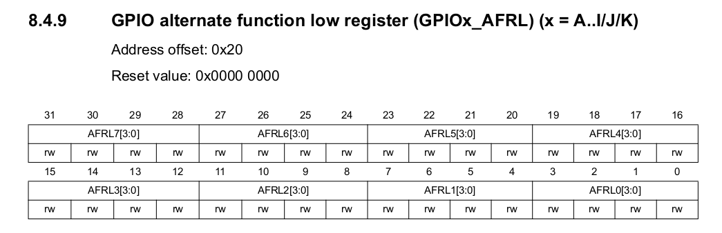
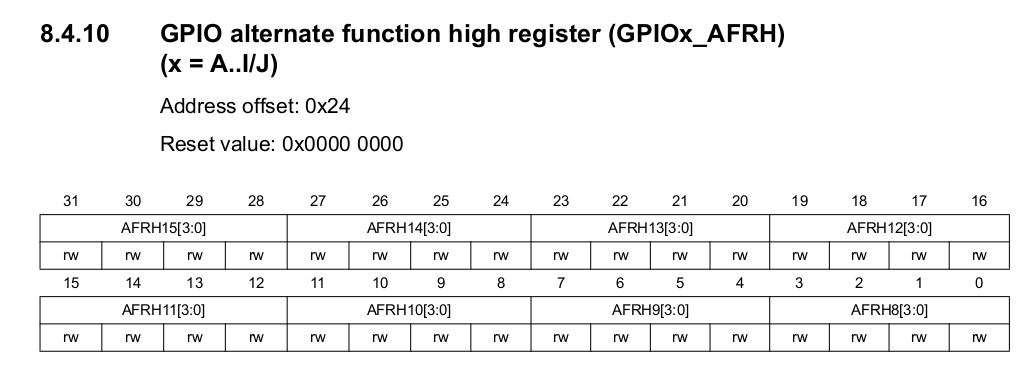
For every port in the MCU these two register exist. To map PA2 to AF1 as in our example, we have to use the bit mapping underneath the register description:
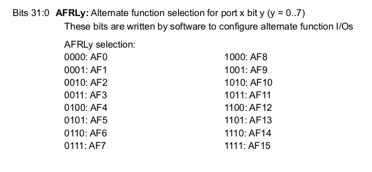
AF1 is represented by bit pattern 0b0001. So we set port A (x), bit 2 (y) by writing 0b0001 into this register:
GPIOA->AFR[0] |= (0b0001 << 4);
Explanation:
- 0b0001: Bit pattern to be set,
- 4: nmuber of bits to be shifted (must end up in bit 7:4)
Hint: You will often find that register labels in the respective .h-file are inconsistent. The two branches of AFR-register (AFRL and AFRH) in this case are not named as they appear in reference manual but are named AFR[0] and AFR[1]. Sometimes it just helps to check the include file for this if compile fails due to a non-recognized identifier.
2 Example
For a practical example of how to use the AF register, we will get back to the last lesson, where we dealt with clocking the CPU. STM32 MCU incorporates a technique to connect some of the clocks to an external pin and therefore measure its frequency. We will take advantage of this.
Basic information: In the STM32 it is possible to hand out the clock signal to a pin. This is called “MCO” (master clock out). When you check the AF-table on p. 62 of the datasheet, you will recognize this portion:
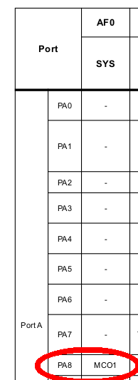
With this information we can deduce that activating MCO to PA8 requires switching AF0 in AFR[0] register because AF0 is in the first block of possible AF address space (from AF0 to AF7).
The respective code is as follows:
//Turn on GPIOA
RCC->AHB1ENR |= RCC_AHB1ENR_GPIOAEN; //RCC->AHB1ENR |= (1<<0);

//Set PA8 as MCO pin
RCC->CFGR |= (0b11 << 21); //MCO1: Microcontroller clock output 1 11: PLL clock selected
RCC->CFGR |= (0b100 <<24); //Divide f.out by 2
GPIOA->MODER |= (2 << (8 << 1)); //PA8 as AF
GPIOA->OSPEEDR |= (3 << (8 << 1)); //HiSpeed
GPIOA->AFR[1] = 0; //0b0000
Explanation:
After activation of GPIOA the next code line sets bit22 of the RCC-CFGR register. This will put out the PLL clock generated signal to MCO output.
After that we divide the frequency by 2 which is basically not necessary in this case because the pin can handle f.max=100MHz. So, this is just for demonstration.
Next line (#3 in this sequence) activates AF for PA8.
Line #4 sets output port speed to max. value.
The last line in the sequence maps MCO output PA8 by activating AF0. This means writing 0b000 to the first 4 bits of AFR[0] register.
With this you’re done again.
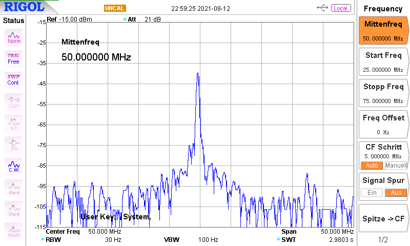
The example can be downloaded from my Github repo.
When connected to a spectrum analyzer you can identify a 50MHz signal on the screen (50MHz = 100Mhz / 2):
Thanks for attending this lesson!
All rights reserved by Peter Baier, Bad Bergzabern, Germany (https://micromaker.de).