0 Abstract
SPI (serial peripheral interface) is a communication interface between electronic devices like microcontrollers, displays, DDS generators and many other electronic circuits. It is widely used, thus the manufacturers of microcontrollers have implemented predefined SPI functions into their hardware. On the other hand, it is possible (and easy) to write these functions on your own. Sometimes this is the even preferably way because debugging is easier and faster. But today we will focus on using the integrated SPI hardware found in the STM32 MCUs.
1 SPI: The basics in brief
SPI uses 3 or 4 lines between the so called “host” (often called ‘master’) and the peripheral device (often named “slave”).
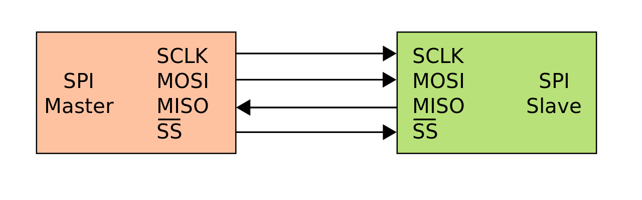
(from Wikipedia)
In the datasheet of any SPI device you can find something that is called “timing diagram”. They all look much or less the same, SPI is standardized to a very high degree.
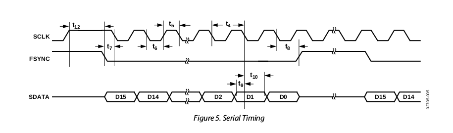
(from datasheet AD9834, an Analog Devices DDS synthesizer)
The first line represents the so called “clock signal”, it switches from low to high, indicating that the current data bit is to be read right in that very moment (line #3). The data stream that goes from master to slave is called MOSI” (“master out, slave in”).
The remaining signal to be explained is called “CS” (for “chip select”, sometimes named differently like “FSYNC” in that case or “NSS” for “negative slave select” in ST’s language). It indicates that the master has got data now for the peripheral device and that it should listen to it. If you have more than one “slave” device in your circuitry you must have a separate CS line for every “slave” in case you do not use cascaded slaves. CS, by the way, is an “active low” signal line.
A fourth line is the “MISO” (master in slave out) line which transfers data from “slave” to “master”, if requested.
2 Setting up SPI in the STM32 microcontroller
There are up to 3 SPI devices in the STM32F4 MCU and they are controlled, again, using the “alternate function” mapping.
Hint: A warning is given in the reference manual by STM because some SPI pins interfere with other essential functions like the JTAG interface for example. See page 873 of the reference manual for details! Any interference in this area might hinder your application from functioning!
In our following code discussion we will use SPI2 which is not prone for any of these conflicts.
Setting up the peripheral SPI structure
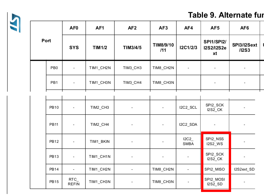
Here you can recognize that the relevant pins are PB15:PB12. Thus we have to start with powering and clocking the respective port, i. e. GPIOB as well as clocking the SPI
//////////////////////////////////////////
// Setup SPI
//////////////////////////////////////////
//PB12:CS; PB13:SCK; PB14:MISO; PB15:MOSI
RCC->AHB1ENR |= (1 << 1); //GPIOB power clock enable
RCC->APB1ENR |= (1 << 14); //Enable SPI2 clock, bit 12 in APB2ENR
Next we set up port B:
//Alternate function ports
GPIOB->MODER &= ~(0b11111111U << (12 << 1)); //Reset bits 15:12
GPIOB->MODER |= (0b01 << (12 << 1)); //PB12 (CS) as output
GPIOB->MODER |= (0b101010U << (13 << 1)); //Set bits 15:13 to 0b101010 for alternate function (AF5)
GPIOB->OSPEEDR |= (0b11111111 << (12 << 1)); //Speed vy hi PB15:PB12

//Set AF5 (0x05) for SPI2 in AF registers (PB13:PB15)
GPIOB->AFR[1] |= (0x05 << (20)); //PB13
GPIOB->AFR[1] |= (0x05 << (24)); //PB14
GPIOB->AFR[1] |= (0x05 << (28)); //PB15
There is some confusion about the CS line in many publications. It is recognized that SPI is little bit faulty in the STM32s. This affects CS (NSS) signal. A workaround is to define this line as “normal” output and switch it by software when transmitting data.
The second block sets the “alternate function registers” according to the table above an the AFR[1] register. If you aren’t quite clear about this technique, please refer to lesson 4 where AF usage is explained in detail.
After having done port configuration the last remaining step is to specify the working conditions for the SPI interface:
//Set SPI2 properties
SPI2->CR1 |= (1 << 2); //Master mode
SPI2->CR1 |= SPI_CR1_SSM; //Software slave management enabled
SPI2->CR1 |= SPI_CR1_SSI; //Internal slave select The value of this bit is
//forced onto the NSS pin and the IO value of the NSS pin is ignored.
SPI2->CR1 |= SPI_CR1_SPE; //SPI2 enable
With this you are done with preparing the SPI interface and can start transmitting data:
void spi_write(uint8_t data)
{
    GPIOB->ODR &= ~(1 << 12); //CS low
    SPI2->DR = data; //Write data to SPI interface
    while (!(SPI2->SR & (1 << 1))); //Wait till TX buf is clear
    GPIOB->ODR |= (1 << 12); //CS high
}
As code examples there are three files to illustrate basic SPI application:
#1: The basic procedure that can be seen above and that has been explained (hopefully) to the details (Link to file)
#2 An example that shows the basic driving functions for a typical SPI LCD (IL9341). This code lacks extensive functions, it just holds an initialization and a clearscreen routine. (Link to file)
#3 A full display driver for the ILI9341 containing all the functions you need to drive this display in text mode (including various character sizes) (Link to file)
Have a good one!
All rights reserved by Peter Baier, Bad Bergzabern, Germany (https://micromaker.de).