0 Abstract
In this lesson we will talk about port configuration in the STM32F4 MCU. First a closer look to a thing called “registers” will be taken and later we will cover first output port configuration. By the end of this lesson input port config and usage will be discussed.
1.0 Handling registers
When reading and writing data inside a microcontroller, in 100% of the cases registers have to be accessed. Like registers have names (“abbreviations” or acronyms to say more precisely). They are defined in a large header file you can find in the CMSIS-folder in your working environment.
Important: These acronyms often correspond 100% with the names in datasheet or reference manual. But sometimes they don’t! We will give hints when this is the case with a certain register.
Registers are part of an overlaying structure. For example the structure called “General-purpose I/Os (GPIO)” contains registers that are called “MODER” (mode register), “ODR” (output data register), “IDR” (input data register) an so on.
In C++ registers are accessed via the “->” operator:
Example: GPIOA->MODER = 0x001 assigns the value of “1” to the mode register of port A. The “->” operator is equivalent to the “.” operator but that can not be used here.
All registers are declared and defined in the various header files and C-definitions for the respective MCU model.
1.1 Exemption: Accessing registers by address
In the rare cases where no acronym exists and a register is not declared/defined in CMSIS file you have to access this location by its memory address. So this hint might be helpful.
Example: Reading flash memory size from its respective register:
In an STM32F411 flash memory size is stored as read-only value in 16-bit register with address 0x1FFF7A22. To read it you can use the following code:
uint16_t (*flashsize) = (uint16_t*)(0x1FFF7A22);
Explanation: A 16-bit pointer variable named *flashsize is declared and defined as the content of memory cell 0x1FFF7A22. The content of this memory cell then is read as a 16 bit variable.
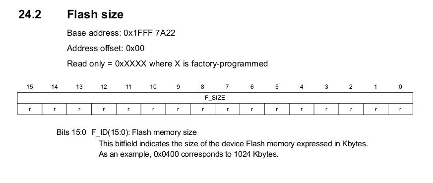
(Source STM32F411 datasheet, p. 839)
1.2 Using I/O ports
A main basic concept for STM32 MCUs compared is that the various units in the processor all have to be powered up separately because this saves energy consumed by the unused ports of the MCU. If you don’t use it, switch it off! Or, to say in more exactly: Don’t switch it on! This concept at first might irritate the experienced AVR developer because a software will simply not work because you forgot to power up the respective port, module or whatever by accident.
Important hint: Like in other MCUs you are not gaining full access to all ports because some of them hold functions that are prioritized for programming the MCU and for debug purposes. These are
PA13, PA14, PA15, PB3 and PB4
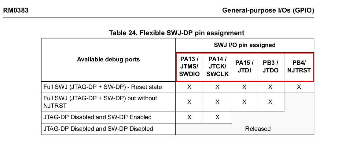
They can be remapped as standard I/O ports but you will lose functionality. For instance you won’t be able to program your MCU again because it will not communicate with your programmer anymore. In this case, to be able to re-flash the MCU’s memory hold the RESET button on your board, release it and in the same second start the upload. But change the code before to prevent running into the same trap.
1.2.1 Powering up a port
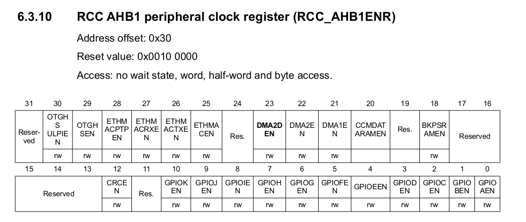
In the STM32F4 there are a number of registers that define the power and clocking status of the hardware. The registers that are needed here are called the RCC-register section (Reset and Clock Control). In the reference manual you will find them beginning with page 161.
The register that is needed from this section if you want to power up an I/O port is called the AHB1ENR-Register which stands for APB1 peripheral clock enable register. APB1 is one of the bus systems of the MCU.
Hint: When you see an underscore “_” in the STM reference manual when describing register access, you will code the “->”-operator in your “real world” program. The “->”-operator in this example refers to a member called “AHB1ENR” of the “RCC” struct. An equivalent expression would be (*RCC).AHB1ENR. But as nobody does that we won’t do it either as mentioned before.
Register AHB1ENR is the register that is used to power up ceratin parts of the MCU. Among are all the GPIOs (ports) from A to K max. (depending on the MCU you have in use).
The instruction to power up port A for example can look like
RCC->AHB1ENR |= RCC_AHB1ENR_GPIOAEN;
The bold “A” marks the port ID and the numeric constant defined in the .h-file for this MCU named by #include “stm32f4xx.h” in a subfolder of the “CMSIS”-folder that has been installed with the programming software.
Or the instruction can be more cryptic in the style of a bit shift operation:
RCC->AHB1ENR |= (1 << 0);
No matter which syntax you use, you set bit 0 of the register to “1” which enables the port (see register description above!).
With this instruction your port is powered up. Next you have to define the port’s function:
1.3 Define what the port will be used for
All ports are defined in the GPIO structure (General Purpose Input Output) of the MCU model. Every port has its own GPIO, beginning with GPIOA, GPIOB etc.
Port mode register (MODER)
With this register you can define a specific pin of port as:
- Input
- Output
- Alternate Function
- Analog mode
Which might be new to AVR users is the so called “alternate function” mode. Many ports, like in the AVR environment, have special functions besides their normal port functionality. We will talk about that topic later because it requires some deeper understanding.
Every port has a 32-bit register to define the function of every pin. The register used is called “MODER” (“mode register”). For port A it is called GPIOA->MODER e. g.:
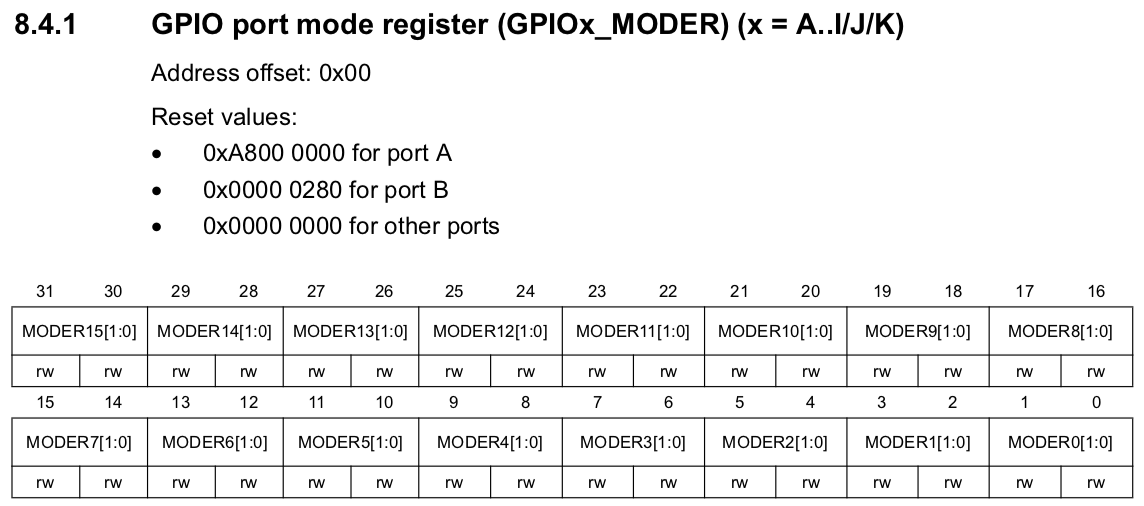
Every pin, in contrast to AVRs, is defined by a 2-bit structure. The respective bit patterns are:
(Source: Internet, unknown)
If you want to set a respective pin to be set as output pin you must write “01b” to the respective bits. BTW: all register are initialized to 0 at start up.
1.3.1 Examples
GPIOA->MODER |= (1 << (3 << 1));
sets pin 3 as output. The inner set of parenthesis multiplies the pin bit (3) by 2 (due to the 2-bit structure) by shifting it on bit left (i. e. *2) and writes the value 1 into that position. This pin is configured as output now.
GPIOA->MODER |= (3 << (5 << 1));
sets pin 5 to analog mode (11b). Which function then exactly is meant has to defined later in a further step. The inner set of parenthesis multiplies the pin bit (5) by 2 again (due to the 2-bit structure) and then writes the value 3 (11b) into that position.
Hint: There also “magic words” for the definitions. You can sometimes see them in example code and find them in the .h-file called “stm32f4xx.h”. We will use register based bit shift operations here.
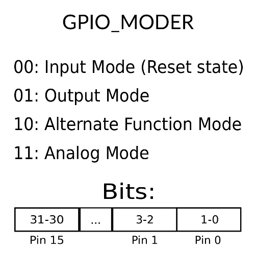
1.4 Defining electrical characteristics of an output port (PUPDR)
This step defines the way of how the port drivers are switched using the PUPDR (pull-up/pull-down-register). This is important when using a pin as input source. You have 3 options available:
00b is neither pull-up or down so the output runs free, 01b pulls the port up to VDD when set to “1”, 10b pulls it down to GND when set. Normally you can leave out this step.
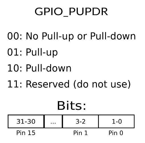
1.5 Setting port speed (OSPEEDR)
As a beginner to STMs you don’t have to care too much about port speed and don’t need to define expressively. But here are the definitions for the various speed levels:
Because “low speed” is set with 00b you don’t have to define anything if you want to use the respective port with this speed.
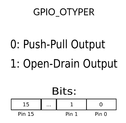
1.6 Setting output driver type (OTYPER)
With the “output type register” your options are to select between Push-pull and open drain. Usually we use predefined state 00b.
Let’s sum it all up: If you intend to set port E pin 0 for example as output the following 2 lines of code are suffice:
//Turn on the GPIOE peripheral
RCC->AHB1ENR |= (1 << 4);

//Put pin PE0 in general purpose output mode
GPIOE->MODER |= (1 << 0);
If you wish to have it in full with all the options available, you might like this example:
//Turn on the GPIOE peripheral
RCC->AHB1ENR |= (1 << 4);

//Put pin PE0 in general purpose output mode (2 bits count!)
GPIOE->MODER |= (1 << (0 << 1));

//Put pin PE0 in general purpose output mode pull UP (2 bits count!)
GPIOE->PUPDR |= (1 << (0 << 1));

//Set speed to high (2 bits count!)
GPIOE->OSPEEDR |= (3 << (0 << 1));

//Set output type to push pull (1 bit count!)
GPIOE->OTYPER &= ~(1 << 0);

Note that

GPIOE->OTYPER |= (0 << 1);

will not work as it does not reset the bit!
1.7 Accessing output ports
Every port has two registers to control data flow: The “ODR” (out data register) and the “IDR” (in data register”). For setting a port we use the ODR:
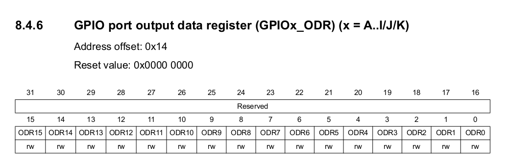
As you can recognize this register has a width of 32 bits as well but only 16 bits (15:0) are used. This makes sense because every port has got 16 pins.
//Reset pin
GPIOE->ODR &= ~(1 << 0);

//Set pin
GPIOE->ODR |= (1 << 0);
This coding might look familiar to AVR programmers.
1.8 Full code example
To come to end of today’s lesson, a full example of setting ports with the STM32F4 can be found on my Github repo.
2 Using ports as input
The code sequence for reading a key looks like one mentioned below. PE4 will be selected as input. This code applies for the F407VGT board by “DIYmore”, for other hardware it is subject to adaption respectively.
//Pin PE4 must be set to 'input' mode with pull-up.
GPIOE->MODER &= ~(3 << (BTNPIN << 1)); //Set to 00b -> Input mode
GPIOE->PUPDR &= ~(3 << (BTNPIN << 1)); //Reset to 00b first
GPIOE->PUPDR |= (1 << (BTNPIN << 1)); //Set to 01b -> Pull up
Decoding input pin is done as follows:
#define BTNPIN 15 //PD15
...
pin_input = ~(GPIOD->IDR); //"0" means "pressed"!
if(pin_input & (1 << BUTTON_PIN))
{
    GPIOE->ODR &= ~(1 << 0);
}
else
{
    GPIOE->ODR |= (1 << 0);
}
The full example can be downloaded here.
Have fun programming and thanks for attending this lesson!