Abstract
An alternative method of generating frequency modulated radio signals will be presented. This project is part of a commercial project and intended for implementing an AFS/FSK data transmission line for exchanging weather data from various stations to a master station with in the 2.4 GHz frequency spectrum. As receivers for narrow band FM were already installed, the transmitter had to use this modulation method as mandatory requirement.
Theory
Data transfer via radio frequency uses different methods. Usually a spectrum of frequencies is transmitted via the radio channel. In the ultimate simple case this is done by just switching the transmitter on and off defined by an underlying coding scheme. One example for this is Morse code. More enhanced modes use at least to distinct frequencies, like in teletyping for example, called “Mark” and “Space”. And higly advanced techniques take advantage of a wider spectrum of subfrequencies thus enhancing data rates massively.
Frequency modulation
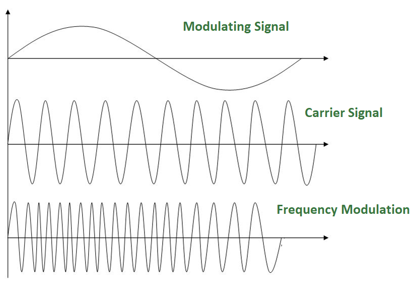
When applying frequency modulation (FM) a given carrier frequency (f0, marked as (ii)) is deflected from its center frequency by adding or subtracting a certain amount of differential frequency (delta.f) depending on the modulated audio signal (af, marked as (i)). FM therefore is one type of a set of angle modulations, like phase modulation (PM) for example. The variation in frequency by time depends on frequency and volume of the modulated signal. A carrier in the HF, VHF, UHF or so spectrum is deflected from its center frequency according to a modulating signal.
Source: https://www.omnisci.com/technical-glossary/frequency-modulation
In a “classical” approach FM is produced by feeding the audio signal into an oscillator using a controlling element that is frequency depending. Popular examples for this type of application are varicap diodes (varactors). Thus a “VCO” (voltage controlled oscillator) is the classical and widely used method of an FM generator in radios. For this experiment we want to use a DDS oscillator instead.
When going along with DDS (direct digital synthesizer) systems, another approach looked sensible when taking into account that high bus data rates are possible with modern DDS chips, particulalry when they are driven in parallel mode. Several possibilities have been described on the internet so far, among one of the manufacturer of DDS modules, Analog Devices.
Fast FM DDS with STM32F4/ARM-Cortex M4 MCU
As microntroller unit in this project we use an STM32F411 MCU clocked to its maximum speed of 168MHz. As DDS an AD9850 by Analog Devices has been applied. The AD9850 not only offers a serial interface (SPI) which is quite common with these devices but also provides a parallel 8-bit mode data transfer. This enhances data exchange rates by factor of 8 compared to serial SPI mode which should make direct modulation possible.
As MCU hardware a so called “Black Pill” board has been purchased carrying the STM32F411. The AD9850 comes from one of the Chinese made ready-to-use boards. These boards already have all the necessary components integrated, including a 125MHz crystal oscillator. Thus all hardware runs on maximum speed.
The interconnections between MCU and DDS are:
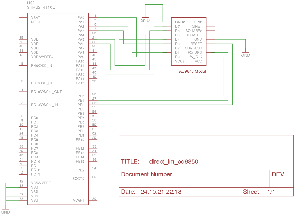
Driving the AD9850 DDS IC via the parallel interface multiplies speed by around the factor of 8. To our experiments this is sufficient for transmitting modulation frequencies in the range of up to 50kHz.
Software
In the following section the software will be described. We have excluded all the customer-specific code not violate the interests of our customer. Wie will talk only about the basic engineering for the project.
Coding demonstrated and explained
The code is divided into several blocks using register oriented programming. As STMF411 (ARM Cortex(R) M4) MCUs are not “fused” like AVRs e. g. This means that user coded software after having run start-up routines needs to set the internal hardware to the desired clock speed. The “Black Pill” board clocks the MCU with a 25 MHz crystal which is referred to as “HSE” (high speed external). The code lines set various PLLs within the MCU to the appropriate division factors thus generating the desired clock frequencies for the single MCU sections. This is a fairly complex process, thus reading of datasheet and reference manual is recommended for better understanding.
//////////////////////////////////////////////
// Set SystemClock to 168 MHz with 25 MHz HSE
//////////////////////////////////////////////
FLASH->ACR |= 0b010; //2 wait state for 100 MHz
RCC->CR |= (1 << 16); //Activate external clock (HSE: 8 MHz)
while ((RCC->CR & (1 << 17)) == 0); //Wait until HSE is ready

//Configuration of PLL
RCC->PLLCFGR |= (1 << 22); //PLL source is HSE

//Set PLLM
RCC->PLLCFGR &= ~0x3F; //1st Reset bits
RCC->PLLCFGR |= 20; //2nd define VCO input frequency = PLL input clock frequency (f.HSE) / PLLM with 2 ≤ PLLM ≤ 63
//-> f.VCO.in = 25MHz / 8 = 1.25MHz

//Set PLLN: PPLLN defines VCO out frequency
RCC->PLLCFGR &= ~0x7FC0; //1st Reset bits 14:6
RCC->PLLCFGR |= (160 << 6); //2nd define f.VCO.out = f.VCO.in * 160 = 200MHz

//Set PLLP: Main PLL (PLL) division factor for main system clock; Reset Bits 17:16
RCC->PLLCFGR &= ~(0b11 << 16); //Reset bits 17:16
//f.PLL.output.clock = f.VCO.out / 2 = 100MHz

//Set PLLQ. PLLQ = division factor for USB OTG FS, SDIO and random number generator clocks
RCC->PLLCFGR &= ~(0b1111 << 24); //Reset bits 27:24
RCC->PLLCFGR |= (8 << 24); //PLL-Q: f.VCO.out / 8 = 25MHz

RCC->CR |= (1 << 24); //Activate PLL, Bit 24
while ((RCC->CR & (1 << 25)) == 0); //Wait until PLL is ready Bit 25

//Division of clock signal for bus system
RCC->CFGR |= (0b1001 << 4) //AHB divider: 100MHz / 4 = 25 MHz
| (0b100 << 10) //APB1 divider: /2
| (0b100 << 13); //APB2 divider: /2

RCC->CFGR |= 0b10; //Switching to PLL clock source
After this we are nearly already done, but DDS ports have to be configured before as output sources:
//////////////////////////////////////////
// Setup DDS
//////////////////////////////////////////
//Turn on the GPIOA peripheral for DDS
RCC->AHB1ENR |= (1 << 0); //GPIOA enable
RCC->AHB1ENR |= (1 << 1); //GPIOB enable

//Put pin A0..A7 in general purpose output mode (DATA-Port)
for(t1 = 0; t1 < 8; t1 ++)
{
    DDS_DATA_GPIO->MODER |= (1 << (t1 << 1));
    DDS_DATA_GPIO->OSPEEDR |= (3 << (t1 << 1));
}

//Put pin B0..B2 in general purpose output mode (CTRL-Port)
DDS_CTRL_GPIO->MODER |= (1 << (W_CLK << 1));
DDS_CTRL_GPIO->OSPEEDR |= (3 << (W_CLK << 1));
DDS_CTRL_GPIO->MODER |= (1 << (FQ_UD << 1));
DDS_CTRL_GPIO->OSPEEDR |= (3 << (FQ_UD << 1));
DDS_CTRL_GPIO->MODER |= (1 << (RES << 1));

//Reset AD9850
DDS_CTRL_GPIO->ODR |= (1 << RES); //Bit set
delay_us(1000); //wait for > 20ns i. e. 1ms minimum time with _delay_s()
DDS_CTRL_GPIO->ODR &= ~(1 << RES); //Bit erase

set_frequency(f);
set_frequency(f);
Main loop now transfers the numerical values of a sine wave to the output port thus generating the desired frequency shifted by a certain functional value of the sine wave. The correct shift rate has been fixed in our radio frequency lab on the basis of numerous experiments.
while(1)
{
    while(t1 < 360)
    {
        set_frequency(f + sine[t1]);
        t1 += 5;
    }
    t1 = 0;
}
Variable t1 in this case is a shift factor that will use the 360 distinct values of the sine wave array with a certain increment that eventually determines the frequency audible in the receiver.
Full code including functions here not pointed out for this experiment can be found in the full code example on Github.
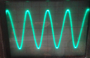
Results
Using a narrow band FM receiver we can read a signal that is is pure sine wave without any noticeable distortion. Audio frequency is about 1 kHz.