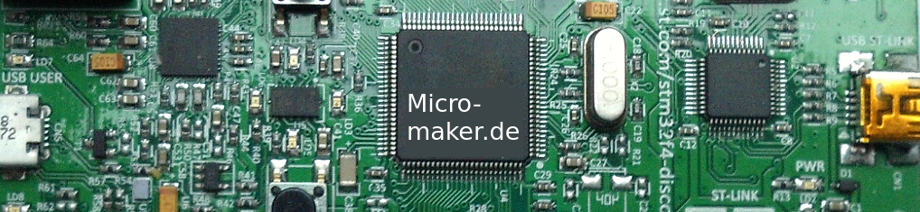
Abstract
I²S stands for “Inter-integrated sound”. It is a standard interface for driving sound hardware that is dedicated to drive special supporting a respective data format. For this tutorial we will use an original STM42F4 “Discovery board” hence it has a sound chip on board that supports I²S: The CS43L22 sound module manufactured by Cirrus Logic (CL). We will demonstrate in a relatively simple way of transferring audio data to the CL-chip and show how registers must be set in advance.
I²S theory
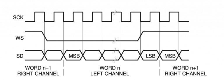
I²S consists of two different ways to access the sound chip: First is a standard I²C interface transferring digital data to perform register settings to prepare later usage of the module. The second interface is a more or less “analog” one, where sound data is written into the sound chip as “analog” values even if they are coded digitally as 16-bit values. I2S has been created by Philips company as a transfer system for two-channel stereo audio streams. The left respectively the right channel audio data is defined by the state of signal called “WS” (word select). This signal is generated by the STM32-built in I²S interface.
I²S data transfer and timing
Data transmission starts with MSB. Due to the fact that data length might differ from 32 down to 8 bits the ending of the “word” must be marked. This is the switching noticeable on the “WS” line. The line switches on clock cycle before “WS” changes from “hi” to “low” or vice versa. This clearly marks the ending of the data word. WS “low” means “left channel”, WS “high” stands for “right channel” data. As you might notice the whole data structure resembles to something very familiar. The lines are very much like the ones in an SPI interface setup. A clock line (“SCK”) is also present as well as a data line (“SD”). Usually the interface is setup for the master to supply the clock signal.
I²S in an STM32F4 microcontroller
The information concerning I²S interface can be found in the STM407 reference manual together withe the information on SPI starting with page 873. Both interfaces share some of the hardware as common. Some registers are for SPI only, by the way.
A simple example for I²S usage
A very basic example code for this complex topic is on our Github repo. To keep fuss to a low level, no “extra features” like DMA etc. have been implemented. The code consists of various sections which will be explained in brief:
- A definition of a sine wave
- A set of functions for I²C communication used for register setting
- Some functions for configuring the sound chip (cs43_enable_right_left(), cs43_set_volume(), cs43_start() and cs43_stop())
- …and the main() function
Initializing the sound chip using I²C
This function starts with setting system clock to max. speed. Next step is to configure PB6 and PB9 as I²C lines for setting sound chip registers. After that the sound chip is put into reset. After resetting the chip a set of standard register values is set to ensure proper function for our demonstration. It is recommended to refer to the sound chip’s datasheet for further reading
Initializing the MCU ports for I²S
This is not trivial, so we have to go into the details:
/////////////////////////////////////////////////////////////////
//Configure I2S-Ports for I2S_MCK, I2S_SCK, I2S_SD, I2S__WS
/////////////////////////////////////////////////////////////////
RCC->AHB1ENR |= (1 << 2); //Enable PORTC
GPIOC->MODER |= (2 << (7 << 1)); //I2S_MCK PC7 (AF)
GPIOC->MODER |= (2 << (10 << 1)); //I2S_SCK PC10 (AF)
GPIOC->MODER |= (2 << (12 << 1)); //I2S_SD PC12 (AF)
RCC->AHB1ENR |= RCC_AHB1ENR_GPIOAEN; //(1 << 0); //(Re)enable PORTA
GPIOA->MODER |= (2 << (4 << 1)); //I2S_WS PA4 (AF)

//Set AF-registers
GPIOC->AFR[0] |= (0b0110 << 28); //PC7 AF6
GPIOC->AFR[1] |= (0b0110 << 8); //PC10 AF6
GPIOC->AFR[1] |= (0b0110 << 16); //PC12 AF6
GPIOA->AFR[0] |= (0b0110 << 16); //PA4 AF6
There are various I2S function block accessible on this MCU.
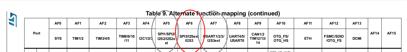
I²S register in STM32F4
First PORTC is enabled because we want to use I2S3 (marked in red) coded as AF6. The ports are designated to the various lines as:
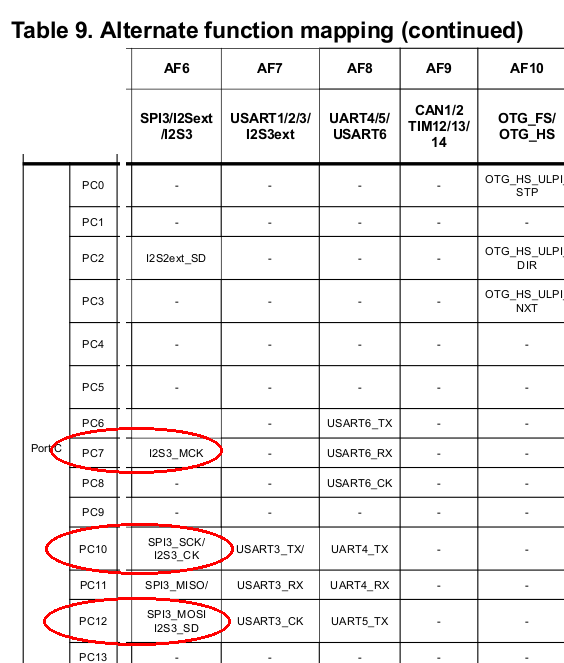
Not shown here is PA4 that is the WS line for I2S3 (see page 62 of datasheet!) Next some more basic settings are made using the SPI registers of the MCU that also are applied for I2S definitions. See the comments for gaining knowledge about what each line’s purpose is.
/////////////////// //Configure SPI3 ///////////////////
RCC->APB1ENR |= (1 << 15); //Enable SPI3 clock
SPI3->I2SCFGR |= (1 << 11); //I2S mode selected
SPI3->I2SCFGR |= (2 << 8); //Master TX
SPI3->I2SCFGR &= ~(2 << 4); //Standard Phillips
SPI3->I2SCFGR &= ~(2 << 2); //Data format 16 bits
SPI3->I2SCFGR &= ~(1 << 0); //CHLEN=16 bits
SPI3->I2SPR |= (1 << 9); //Master clock output enable
SPI3->I2SPR |= (2 << 3) | (1 << 8); //Prescaler /8 and ODD-factor=1

//Start PLL for I2S
RCC->CR |= (1 << 26); //PLLI2S on
while(!(RCC->CR & (1 << 27))); //Wait until PLL is ready
SPI3->I2SCFGR |= (1 << 10); //I2S enabled
After this part of code we are ready to transfer data to the sound chip via I²S bus. Sine wave data is transmitted to the sound module using a simple loop:
while(1)
{
    //Build Sine wave, cheap AND dirty, just for demo!
    for(t0 = 0; t0 < 360; t0++)
    {
        for(t1 = 0; t1 < 2; t1++)
        {
           SPI3->DR = wave[t0] << 1;
           for(t2 = 0; t2 < 10; t2++){}; //Delay!
        }
    }
}
At this point you are kindly invited to do further experiments! 🙂 Peter B.
All rights reserved by Peter Baier, Bad Bergzabern, Germany (https://micromaker.de).