0 Abstract
This article will demonstrate how an Si5351 clock oscillator (made by Silicon Labs) is controlled using I²C bus connected to an STM32F4 MCU. The method of configuring this chip is relatively complex and will be shown in detail as well as other significant aspects will be discussed.
1 Si5351A clock oscillator basics
Si5351 is a product by Silicon Labs (“SiLabs”). There are some variants available, which share common basic functions. Differences are in the number of oscillators integrated on one chip. The specific product that will be discussed here, the Si5351A, has 3 output ports (named “OSC0”, “OSC1” and “OSC2”), each individually programmable in the frequency range from 8kHz to 160MHz.
Si5351 is designed for a supply voltage of 3.3V thus making it compatible with the STM32F4 processor without the necessity for voltage shift circuits.
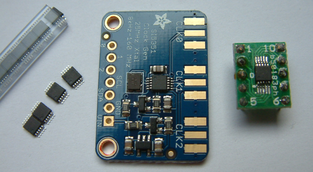
The IC is a 10 pin SMD package (left). There are also breakout boards available that are 5V compatible (Adafruit, center). Or just by converting SMD package to DIL header strips (right):
2 Coding for the Si5351
2.1 Init procedure
To say in advance: Frequency generation with the Si5351 is more complex than with DDS system by Analog Devices. First we have to define I²C settings because the module communicates via the 2-wire interface. To learn about I²C on the STM32-MCU, please refer to out tutorial.
////////////////////////
// Defines for Si5351 //
////////////////////////
#define SI5351_ADDRESS 0xC0 //Check individual module for correct address setting. IDs may vary!
#define FXTAL 27000000 //Hz
#define PLLRATIO 32 //FXTAL * PLLRATIO = f.VCO
I²C address for most Si5351 chips I have encountered is 0xC0. This is defined as well as the clock on board or next to the chip, which usually is 25 MHz for the Adafruit boards. I am using 27MHz instead.
PLLRATIO fixes the PLL frequency which in this case is calculated as 32 * 27 MHz = 864MHz (max. 900MHz according to datasheet!).
The Si5351 clock oscillator has a number of registers whose cells will be filled later with appropriate values. They are also coded as a set of definitions:
//Set of Si5351A relevant register addresses
#define CLK_ENABLE_CONTROL 3
#define PLLX_SRC 15
#define CLK0_CONTROL 16
#define CLK1_CONTROL 17
#define CLK2_CONTROL 18
#define SYNTH_PLL_A 26
#define SYNTH_PLL_B 34
#define SYNTH_MS_0 42
#define SYNTH_MS_1 50
#define SYNTH_MS_2 58
#define SPREAD_SPECTRUM_PARAMETERS 149
#define PLL_RESET 177
#define XTAL_LOAD_CAP 183
As with most complex ICs there is an initialization process required. To get data into the oscillator, we have a function (i2c_write()) for this job. Check the full software code on my Github repo to get the code and also see the I²C section of the tutorial!!
//////////////////////
// Si5351A commands //
//////////////////////
//Set PLLA (VCO) to internal clock rate of 900 MHz
//In this example PLLB is not used
//Equation fVCO = fXTAL * (a+b/c) => see AN619 p.3
void si5351_start(void)
{
    unsigned long a, b, c;
    unsigned long p1, p2;

    //Init
    i2c_write(PLLX_SRC, 0); //Select XTAL as clock source for si5351C
    i2c_write(SPREAD_SPECTRUM_PARAMETERS, 0); //Spread spectrum diasble (Si5351 A or B only!
    i2c_write(XTAL_LOAD_CAP, 0xD2); // Set crystal load capacitor to 10pF (default),
    // for bits 5:0 see also AN619 p. 60
    i2c_write(CLK_ENABLE_CONTROL, 0x00); // Enable all outputs
    i2c_write(CLK0_CONTROL, 0x0E); // Set PLLA to CLK0, 8 mA output
    i2c_write(CLK1_CONTROL, 0x0E); // Set PLLA to CLK1, 8 mA output
    i2c_write(CLK2_CONTROL, 0x0E); // Set PLLA to CLK2, 8 mA output
    i2c_write(PLL_RESET, (1 << 5)); // Reset PLLA and PLLB

    //Set PLLA to 864MHz
    a = PLLRATIO; // Division factor 864/27 MHz
    b = 0; // Numerator, sets b/c=0, See AN169 p.3!
    c = 0xFFFFF; // Max. resolution, but irrelevant in this case as b=0. See AN169 p.3!

    //Formula for splitting up the numbers to register data, see AN619
    p1 = 128 * a + (unsigned long) floor(128 * b / c) - 512;
    p2 = 128 * b - c * (unsigned long) floor(128 * b / c);

    //Write data to registers of PLLA so that VCO is set to 864MHz internal freq
    i2c_write(SYNTH_PLL_A, 0xFF);
    i2c_write(SYNTH_PLL_A + 1, 0xFF);
    i2c_write(SYNTH_PLL_A + 2, (p1 & 0x00030000) >> 16);
    i2c_write(SYNTH_PLL_A + 3, (p1 & 0x0000FF00) >> 8);
    i2c_write(SYNTH_PLL_A + 4, (p1 & 0x000000FF));
    i2c_write(SYNTH_PLL_A + 5, 0xF0 | ((p2 & 0x000F0000) >> 16));
    i2c_write(SYNTH_PLL_A + 6, (p2 & 0x0000FF00) >> 8);
    i2c_write(SYNTH_PLL_A + 7, (p2 & 0x000000FF));
}
Some words on the code: First internal PLL is set to 864 MHz which provides the basic clock inside the module. This value is split up by using the formula from Si5351-AN619, an application note referring to the chip. In AN619 we read (p. 3):
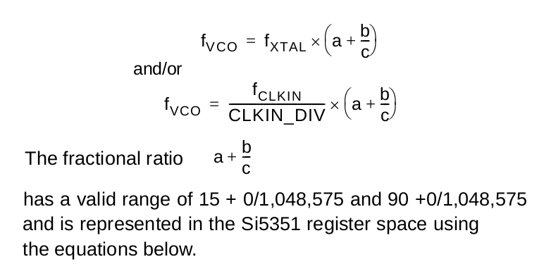
From the first equation we can learn, that by the division factor (a+b/c) any frequency between the give boarders can be set. In this case it is simple as a=32 and b=0. This value is split by a set of calculations into the various registers that hold the value.
2.2 Generating an output frequency
A similar method is used to calculate the frequency settings for an output frequency. This sometimes leads to confusion:
void si5351_set_freq(int synth, unsigned long freq)
{
    unsigned long a, b, c = 0xFFFFF;
    unsigned long f_xtal = FXTAL;
    double fdiv = (double) (f_xtal * PLLRATIO) / freq; //division factor fvco/freq (will be integer part of a+b/c)
    double rm; //remaining
    unsigned long p1, p2, p3;

    a = (unsigned long) fdiv;
    rm = fdiv - a; //(equiv. to fractional part b/c)
    b = (unsigned long) (rm * c);
    p1 = 128 * a + (unsigned long) floor(128 * b / c) - 512;
    p2 = 128 * b - c * (unsigned long) floor(128 * b / c);
    p3 = c;

    //Write data to multisynth registers of synth
    i2c_write(synth + 0, (p3 & 0xFF00) >> 8);
    i2c_write(synth + 1, p3 & 0xFF);
    i2c_write(synth + 2, (p1 >> 16) & 0x03);
    i2c_write(synth + 3, (p1 & 0xFF00) >> 8);
    i2c_write(synth + 4, (p1 & 0xFF));
    i2c_write(synth + 5, (p3 & 0xF0) | ((p2 >> 16) & 0x0F));
    i2c_write(synth + 6, (p2 & 0x0000FF00) >> 8);
    i2c_write(synth + 7, (p2 & 0x000000FF));
}
In AN619 on p. 6 you can find certain equations:
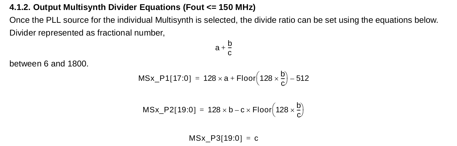
First a divide ratio has to be calculated (magenta line). This is split into the variables a, b and c (set of green lines). Later it is filled into the various registers (blue lines). This defines the output frequency. As b and c build a fraction with a theoretically infinite number of distinct values a very fine frequency adjustment is possible.
To access a respective oscillator the parameter synth is given with the range of 0 <= synth <= 2 fpr the Si5351A oscillator. As always, and as mentioned before, the full example can be downloaded from my Github repository.
CU later!
By Peter Baier (DK7IH)